Materials Needed
Here is the list of the materials that were used for this part of the project:
Part I: Data & Address Bus Demultiplexing
To begin our project, we must first familiarize ourselves with the way a microprocessor works. We will use an Arduino to simulate the use of a microprocessor.

We assume that the microprocessor we are using has an 8-bit data & Address bus. We will use pins AD0 – AD7 to simulate these buses. The microprocessor we are using contains an ALE (Address Latch Enable) which is necessary to demultiplex our buses. Also, the use of the Octal Latch 74LS373 is going to be necessary.
Why should we demultiplex the buses?
It is imperative that the buses are demultiplexed (or separated). Since the microprocessors are small-compact chips; Designers must save space on these chips by using the same pins for different functions. In this case, the pins AD0 – AD7 are used for both the Address Bus (A0 – A7) and the Data Bus (D0 – D7). However, both the Address Bus and Data Bus are multiplexed (combined) – so it is necessary to separate the buses to use them individually. We achieve this separation by using the Octal Latch 74LS373 chip which already contains the ALE.
Data & Address Bus Demultiplexing: Design
Before we can begin the hardware part of our project, it is important to first design and test the circuit we are building to make sure it functions properly. To do this, we will use a software called LogicWorks which can be used to test our design.
As mentioned before, we will use the 74LS373 to demultiplex the buses of the microprocessor. We will also use simple switches to simulate the pins AD0 – AD7. It is important to understand the functionalities of the chips we are using, for example, the 373 contains a control signal (ALE) and it is this control signal that will tell us how the latch is going to work. When ALE has value 1 (HIGH), the input values on the 373 will be latched to the output. This will be the Address Bus. When ALE has value 0 (LOW), the output of the 373 will remain unchanged. The Data Bus will be the input to the 373.
In this LogicWorks design, we will use the EN (Enable) control signal as the ALE and we will not use the OEN (Output Enable) control signal so we can simply ground it. Note: We don’t necessarily have to ground OEN in LogicWorks, however, when we are building the hardware, not grounding this control signal may cause our circuit to not work correctly.
The design will look something like this:
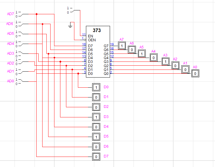
It is important to familiarize ourselves with how the components work and we are encouraged to mess around with the values to fully understand how the chip works. For example, here we see that the output of the 373 in binary is 1010 1000 which is equal to 168 in decimal notation or A8H in hexadecimal notation, this is the value of the Address Bus. Then, we have the input to the 373 which is 0010 1001 in binary (41 in decimal or 29H in hexadecimal), this is the value of the Data Bus.
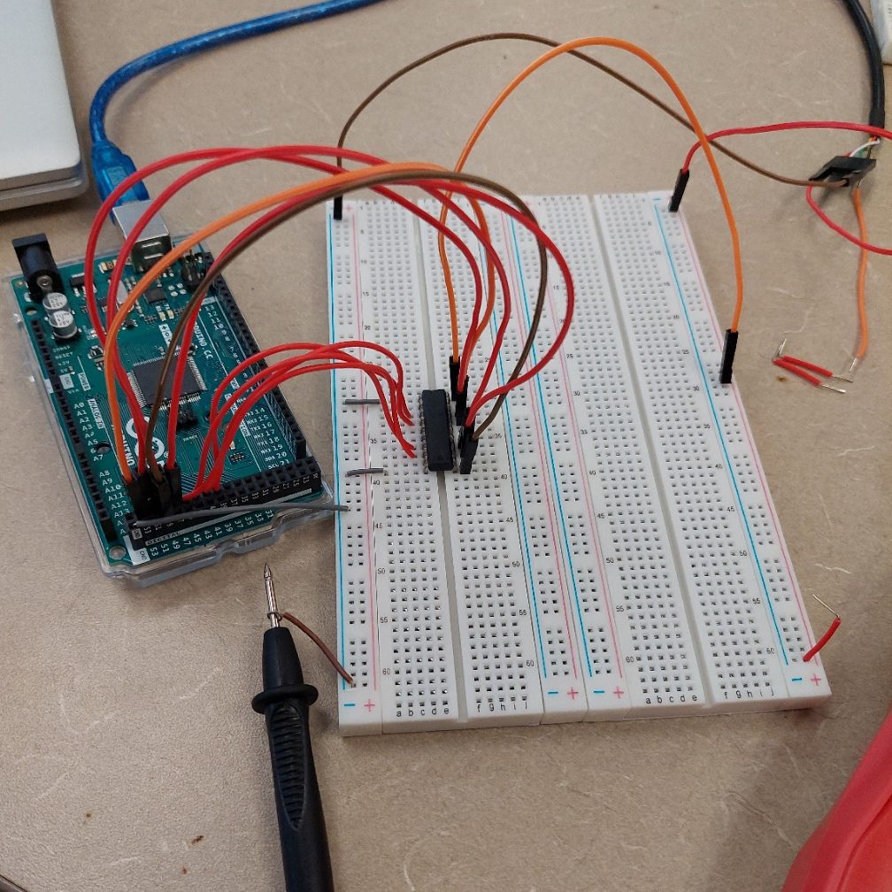
Data & Address Bus Demultiplexing: Hardware
We can now start building our circuit and test our design by hard wiring our LogicWorks circuit on a breadboard. Again, we will use pins AD0 – AD7 on our microcontroller to simulate the microprocessor.
The following pin mapping will be used from the microcontroller to simulate the AD pins:
- 52 – AD7
- 50 – AD6
- 48 – AD5
- 46 – AD4
- 44 – AD3
- 42 – AD2
- 40 – AD1
- 38 – AD0
- 49 – ALE
The Arduino Microcontroller uses 5V to provide power to the circuit, we can simply use any PC or Laptop with a USB port to power to the circuit. We can also connect any 5V battery to the circuit.
Texas Instrument SN74LS373:
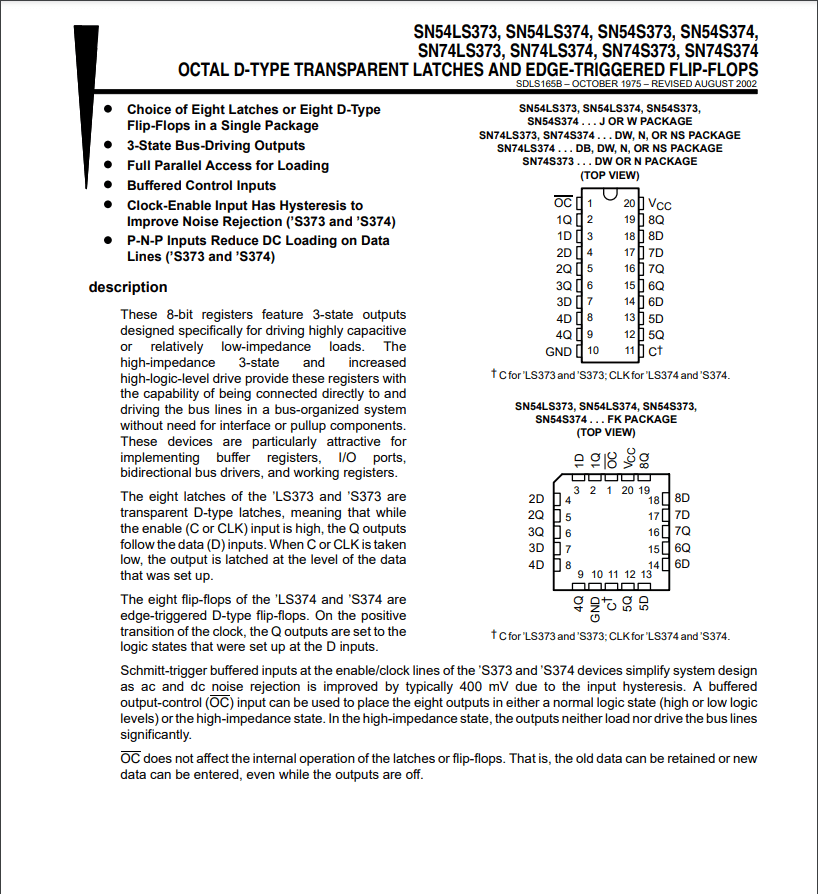
We will use this Data Sheet to follow the pin diagram and make the right connections. Here, 1D-8D represents the input and 1Q-8Q represents the output. Pin 11 is our ALE and OC must be grounded. The pins must be properly connected to the corresponding places, otherwise the circuit might not work.
The circuit will look like this:
Data & Address Bus Demultiplexing: Software
Now that we built our hardware, how can we test it?
We will write the software to test the new circuit we just built. We will be using Arduino IDE to write our code. It is important to understand the different modes in which the pins in the Arduino IDE work. In our software, we can declare an 8-bit array named AD to simulate our pins AD0-AD7.
The software can look something like this, however, there are many ways to do it:
#define PIN_INT 2
//#define PIN_M_IO 51
#define PIN_ALE 49
//#define READ 43
//#define WRITE 45
void setup() {
// put your setup code here, to run once:
Serial.begin(9600);
int ad[8] = {38, 40, 42, 44, 46, 48, 50, 52};
pinMode(49, OUTPUT);
pinMode(52, OUTPUT);
pinMode(50, OUTPUT);
pinMode(48, OUTPUT);
pinMode(46, OUTPUT);
pinMode(44, OUTPUT);
pinMode(42, OUTPUT);
pinMode(40, OUTPUT);
pinMode(38, OUTPUT);
//pinMode(READ, OUTPUT);
//pinMode(WRITE, OUTPUT);
// digitalWrite(READ, HIGH);
//digitalWrite(WRITE, HIGH);
delay(5000);
//digitalWrite(READ, LOW);
//digitalWrite(WRITE, LOW);
digitalWrite(49, HIGH);
digitalWrite(52, HIGH);
digitalWrite(50, HIGH);
digitalWrite(48, LOW);
digitalWrite(46, LOW);
digitalWrite(44, HIGH);
digitalWrite(42, HIGH);
digitalWrite(40, LOW);
digitalWrite(38, LOW);
delay(5000); //Waits 5 seconds
digitalWrite(49, LOW);
digitalWrite(52, LOW);
digitalWrite(50, LOW);
digitalWrite(48, HIGH);
digitalWrite(46, HIGH);
digitalWrite(44, LOW);
digitalWrite(42, LOW);
digitalWrite(40, HIGH);
digitalWrite(38, HIGH);
}
